High-Density Interconnect PCB: Microvia and Blind Buried Via PCB Fabrication Solutions
In today’s rapidly evolving electronics industry, the demand for miniaturized, high-performance, and reliable circuit boards has skyrocketed. Devices from smartphones to advanced medical equipment require high-density interconnect (HDI) PCBs to achieve compact designs without compromising functionality. As a leading China flex PCB supplier, we specialize in high-quality flex circuit manufacturing—from rapid-turn prototyping to full-volume flexible PCB fabrication. Upload your Gerber files now for a fast, reliable quote.
Understanding HDI PCBs and Their Importance
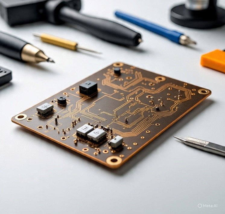
High-Density Interconnect PCBs, commonly known as HDI PCBs, are designed to handle high component density with advanced routing technologies. These PCBs utilize microvias, blind vias, and buried vias to interconnect layers efficiently. Compared to traditional PCBs, HDI boards enable:
- Reduced size and weight of electronics
- Higher signal integrity and faster transmission speeds
- Enhanced reliability for complex designs
From my experience in PCB manufacturing, working with HDI PCBs demands precision and attention to detail. Even minor errors in via drilling or lamination can lead to costly production delays. This is why partnering with a reputable HDI PCB manufacturer ensures that your designs are executed accurately and consistently.
Types of Vias in HDI PCB Manufacturing
Microvia PCBs
Microvias are small, laser-drilled vias that connect adjacent layers in a PCB. Unlike standard through-hole vias, microvias occupy minimal space, allowing engineers to pack more circuits into a smaller footprint. Some key benefits include:
- Compact design for miniaturized devices
- Improved electrical performance
- High reliability under thermal stress
As a microvia PCB manufacturer, we leverage precision laser drilling technology to create vias as small as 75 microns, providing superior connectivity for advanced electronics.
Blind and Buried Via PCBs
Blind vias connect outer layers to one or more inner layers without passing through the entire PCB. Buried vias, on the other hand, connect only inner layers and remain hidden from the outer surface. These via types are essential for multi-layered HDI PCBs because they:
- Optimize board real estate for dense designs
- Reduce signal interference
- Enhance overall circuit performance
In my experience, blind and buried vias significantly improve routing flexibility. However, they require advanced fabrication techniques and rigorous quality control to maintain reliability, particularly in high-frequency or high-current applications.
HDI PCB Fabrication Process
Creating a high-quality HDI PCB involves several precise steps, each critical to the board’s performance:
1. Design and Layout
The process begins with detailed PCB design, including layer stacking, via placement, and trace routing. Using CAD tools, engineers ensure that the high-density interconnect design meets electrical and mechanical requirements. As a leading HDI PCB manufacturer, we collaborate closely with clients to optimize designs for manufacturability.
2. Microvia Drilling
Laser drilling creates microvias with extreme precision. Unlike mechanical drilling, lasers produce cleaner holes with minimal thermal damage. This step is crucial for maintaining the integrity of the board’s signal paths, especially for high-speed circuits.
3. Lamination and Layer Bonding
Multi-layer HDI PCBs require lamination to bond the stacked layers securely. Controlled heat and pressure ensure minimal voids and strong interlayer adhesion. I have observed that meticulous lamination directly correlates with long-term reliability, particularly for boards exposed to thermal cycling.
4. Plating and Copper Filling
Plating the vias with copper ensures reliable electrical connectivity. For blind and buried vias, copper filling prevents potential voids and improves current-carrying capacity. Our microvia PCB fabrication process includes precise copper deposition, providing enhanced durability and conductivity.
5. Testing and Quality Control
Rigorous inspection, including automated optical inspection (AOI) and electrical testing, verifies that the HDI PCB meets design specifications. High-quality HDI PCB manufacturers implement multiple quality checkpoints to prevent defects that could compromise performance.
Applications of HDI PCBs
HDI PCBs are widely used in industries requiring compact, high-performance electronics:
- Smartphones and wearable devices: Microvia PCBs allow for slimmer, lighter devices with improved functionality.
- Medical electronics: HDI boards support miniaturized implants and portable diagnostic equipment.
- Automotive electronics: High-density boards are critical for electric vehicles and ADAS systems.
- Aerospace and defense: Lightweight, reliable HDI PCBs are essential for communication and navigation systems.
From my personal experience, designing HDI PCBs for medical devices requires exceptional attention to detail and adherence to regulatory standards. Each via and trace must be carefully calculated to ensure long-term reliability.
Why Choose Our HDI PCB Manufacturing Services
As a trusted HDI PCB manufacturer, we provide end-to-end solutions tailored to your project’s needs:
- Rapid prototyping: Quick-turn services help test and validate your designs efficiently.
- Full-volume production: High-quality fabrication for large-scale deployments.
- Advanced via technology: Expertise in microvia, blind, and buried via PCBs.
- Flexibility: Capability to handle rigid-flex and multi-layer HDI boards.
- Reliable support: Upload your Gerber files now for a fast, accurate quote.
Our approach combines industry-leading technology with a commitment to quality. From my experience, working with a dedicated manufacturer makes all the difference in delivering HDI PCBs that perform consistently in demanding applications.
Conclusion
The evolution of electronics demands high-density interconnect PCBs that combine compact design, superior performance, and long-term reliability. Whether you need microvia PCBs for compact consumer devices or blind buried via PCBs for complex multi-layer designs, selecting the right HDI PCB manufacturer is crucial.